Micro-EDM
Electrical Discharge Machining
Electrical discharge machining (EDM) is non-contact process capable
of removing material at very small lengthscales without creating
mechanical stresses. The material is removed through highly localized
melting and evaporation as a result of electrical discharges from an
electrode to the material. The discharges, which form tiny plasma
channels with temperatures up to 10,000 °C, locally melt very small
amounts of material. As the plasma collapses when the current flow is
shut off, the resulting vacuum pulls out the molten material into the
surrounding dielectric medium. For discharges to occur, the material
needs to have sufficient electrical conductivity whereas material
hardness is of no consequence. As such, any metal as well as many
semiconductors are candidates for this process.
Micro-EDM is a specialized form of EDM whereby the workpieces have
features as little as 10 microns (0.0004 inches). These small features
are achieved with electrodes that are also very small in size. For EDM
sinker and EDM milling, the typical features are internal geometries
such as holes, slots, etc. Therefore, the electrodes are typically a
tiny bit smaller than the features to be machined. For wire-EDM
(micro-WEDM), where most features are external, this restriction is not
necessarily the case.
 Download
brochure Download
brochure

EDM machinability of various materials (Source: Lee et. a., Effect
of metal coating on machinability of high purity germanium with wire
electrical discharge machining, J Mat Proc 213, 2013)
Micro-EDM Examples - 0.1 mm (0.004 in) brass wire
 |
 |
|
0.4 mm (0.016 in) pitch microelectrode array, 5x5mm (0.2 x
0.2 in) with 144 electrodes of 5 mm height (0.2 in). Material:
doped silicon |
0.4 mm (0.016 in) pitch microelectrode array, 5x5mm (0.2 x
0.2 in) with 144 electrodes of 5 mm height (0.2 in). Cross
section of electrodes is varied along length to increase
flexibility. Material: doped silicon. |
 |
 |
|
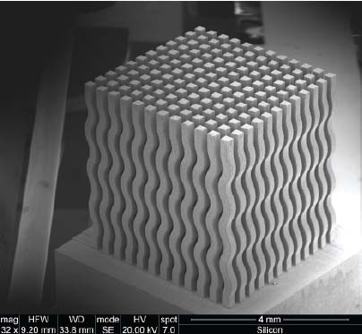
0.4 mm (0.016 in) pitch microelectrode array, 5x5mm (0.2 x
0.2 in) with 144 electrodes of 5 mm height (0.2 in). Cross
section of electrodes is wavy to increase flexibility. Material:
doped silicon |
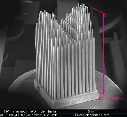
0.4 mm (0.016 in) pitch microelectrode array, 5x5mm (0.2 x
0.2 in) with 144 electrodes of 5-9 mm height (0.2 -0.35 in).
Cross section of electrodes is tapered towards tip to increase
flexibility. Material: doped silicon |
Micro-EDM Examples - 0.05 mm (0.002 in) steel wire
 |
 |
|
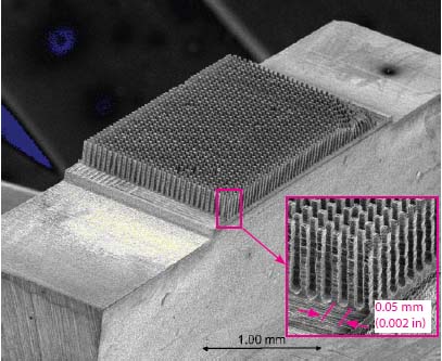
0.15 mm (0.006 in) pitch microelectrode array, 3x3mm (0.12 x
0.12 in) with 1156 electrodes of 1.0 mm height (0.04 in). Cross
section of electrode is curved to increase flexibility.
Material: brass |
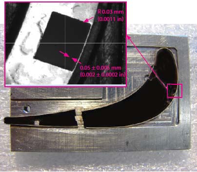
Turbine vane test windows with very small corner radius of
0.03 mm (0.0011 in) and matched curvature as well as very tight
tolerance relative to a non-conductive out layer. Material:
nickel-superalloy. Courtesy of Prof. Kevin Hemker and Binwei
Zhang, Johns Hopkins University. |
Micro-EDM Examples - 0.05 mm (0.002 in) steel wire
 |
 |
|
0.05 mm pitch (0.002) microelectrode array, 1.5x3mm (0.06 x
0.12 in) with 3000 electrodes of 0.2 mm height (0.008 in).
Material: brass |
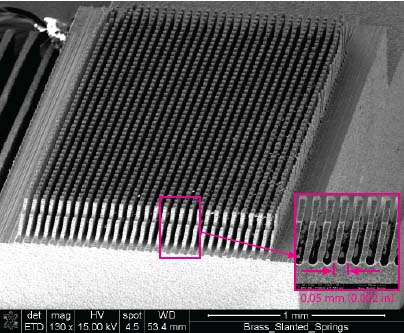
0.05 mm pitch (0.002) microelectrode array, 1.5x3mm (0.06 x
0.12 in) with 3000 electrodes of 0.2 mm height (0.008 in).
Electrodes are slanted to increase electrode flexibility.
Material: brass |
Micro-EDM Examples - 0.012 mm (0.00047 in) tungsten wire
 |
|
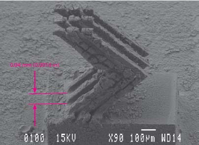
0.04 mm pitch (0.0016) microelectrode array, 0.3x0.3mm
(0.012 x 0.012 in) with 9 electrodes of 0.4 mm height (0.016 in)
- before cleaning. Electrodes have a revere bendslanted to
increase electrode flexibility. Material: copper berylium |
Micro-EDM Examples - rotational features
 |
 |
|
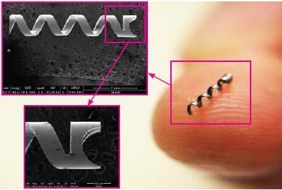
1.0 mm pitch (0.04 in) helical microswimmer machined with
rotary axis. Material: 1mm diameter nitinol tubing. Courtesy of
Prof Jake Abbott, University of Utah |
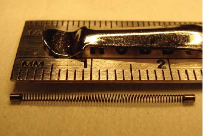
0.3 mm pitch (0.012 in) helix support for artificial
muscles. Material: 1mm diameter nitinol tubing. Courtesy of Prof
Stephen Mascaro, University of Utah |
Further reading
- Experimental investigation of wire electrical discharge
machining of NdFeB permanent magnets with an RC-type machine,
Greer J, Petruska AJ, Mahoney AW, Nambi M, Bamberg E, and Abbott JJ,
Journal of Materials Engineering and Performance 23(4), pp.
1392-1401 (2014).
Download
document here
- Effect of metal coating on machinability of high purity
germanium using wire electrical discharge machining, Lee S,
Scarpulla MA, Bamberg E, Journal of Materials Processing
Technology 213, pp 811- 817 (2013).
Download document here
- Application- specific customizable architectures of Utah
neural interfaces, Sharma R, Tathireddy P, Lee S, Rieth L,
Bamberg E, Dorval A, Normann R, and Solzbacher F, Procedia
Engineering 25, pp 1016-1019 (2011)
- Velocity control with gravity compensation for magnetic
helical swimmers, Mahoney AW, Sarrazin JC, Bamberg E, and Abbott
JJ, Advanced Robotics 25(8), pp 1007-1028 (2011).
Download
document here
- Material removal rate, kerf, and surface roughness of
tungsten carbide machined with wire electrical discharge machining,
Shah A, Mufti NA, Rakwal D, Bamberg E, Journal of Materials
Engineering and Performance 20(1), pp 71-76 (2011).
Download
document here
- Fabrication of high aspect ratio silicon micro-electrode
arrays using micro-wire electrical discharge machining (micro-WEDM),
Rakwal D, Heamawatanachai S, Tathireddy P, Solzbacher F, and Bamberg
E, Microsystem Technologies 15(5), pp 789-797 (2009).
Download
document here
- Slicing, cleaning and kerf analysis of germanium
wafers machined by wire electrical discharge machining,
Rakwal D, and Bamberg E, Journal of Materials Processing
Technology 209(8), pp 3740-3751 (2009).
Download document here
- Electrical discharge machining promises high-quality,
lower-cost substrates, Rakwal D, and Bamberg E, Compound
Semiconductor, March 2009, pp 17-18 (2009)
- Orbital electrode actuation to improve efficiency of drilling
micro holes by micro-EDM, Bamberg E, and Heamawatanachai S,
Journal of Materials Processing Technology 209(4), pp 1826-1834
(2009)..
Download document here
- Experimental investigation of wire electrical discharge
machining of gallium doped germanium, Bamberg E, and Rakwal D,
Journal of Materials Processing Technology 197(1-3), pp
419-427 (2008).
Download document here
|